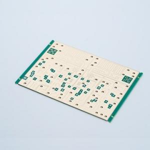
5G module CIRCUIT board FR4 Halogen-free multi-layer pcb with large gold surface
Angel-tech have been focused on research, development and production of precision multi-layer circuit boards, single
double-sided circuit boards, special boards more than ten years.
Our PCB Assembly Capabilities |
| Item | Technical Parameter |
| SMT Jointing Min. Space | 0201mm |
| QFP Space | Pitch 0.3mm |
| Min. Package | 0201 |
| Min. Size | 2*2 inch(50*50mm) |
| Max. Size | 14*22 inch(350*550mm) |
| Placement Precision | ±0.01mm |
| Placement Precision | QFP, SOP, PLCC, BGA |
| Placement Capability | 0805, 0603, 0402, 0201 |
Our factory has introduced and imported excellent production equipments.
Our circuits boards range from double layers to 24 layers.
The product types include ordinary boards, medium and high Tg boards, involving special processes such as semi-hole,
bonding, impedance, blue glue, carbon oil, gold fingers, blind gongs, buried blind holes , Countersunk holes, etc.;
surface treatment can be ordinary tin spray, lead-free tin spray, immersion gold, electro-nickel gold, electro-hard gold,
QSP, immersion silver, immersion tin or composite processes, etc..
Our PCB are widely used in smart electronics, communications Technology, power technology, industrial control,
security engineering, automotive industry, medical control and optoelectronic engineering and other fields.
Specification:
| Base Material | FR4- Halogen-free |
| Permittivity | 4.3 |
| Layer(s) | 4 |
| Board Thickness | 0.80mm |
| Outer copper thickness | 1oz |
| Inner copper thickness | 1oz |
| Mounting Type | Immersion gold & resin plug-hole |
| Min Hole Diameter | 0.28mm |
| Minimum line width | 0.08mm |
| (MLI)Min Line Spacing | 0.08mm |
| Application | Led lights,display screen |
| Characteristic | resin plug-hole,Halogen free, |
| Packaging Details | Inner: vacuum packing or Anti-static package,
Outer: export carton
or according to the customer's requirement. |

Images:
Our PCB factory is fully qualified and has passed a series of certifications including UL, ISO9001, ISO14001,
ISO/TS16949, CQC and so on.
We are a high-tech enterprises is committed to developed by high precision multi-layer circuit boards,allegro and special PCB,
providing customers with fast sample,small and medium batch,mass production.
| PCB Lead time (workday(s)) Normally |
| | Single, Double-sided | 4 layer | 6 layer | Over 8 layer | HDI |
| Sample Lead time (Normal) | 5-6 | 6-7 | 7-8 | 10-12 | 10-12 |
| Sample Lead time (Faster) | 48-72 hours | 5 | 6 | 6-7 | 12 |
| Mass production lead time | 7-9 | 10-12 | 13-15 | 16 | 20 |
| PCB Assembly Lead time |
| Sample Lead time | PCB Fab+Components preparation +PCBA=15 workdays |
| Mass production lead time | PCB Fab+Components preparation +PCBA=21workdays |
Quote Requirement:
*Gerber file of the bare PCB board.
*BOM (Bill of material) for assembly.
*To short the lead time, please kindly advise us if there is any acceptable components substitution.
*Testing Guide & Test Fixtures if necessary.